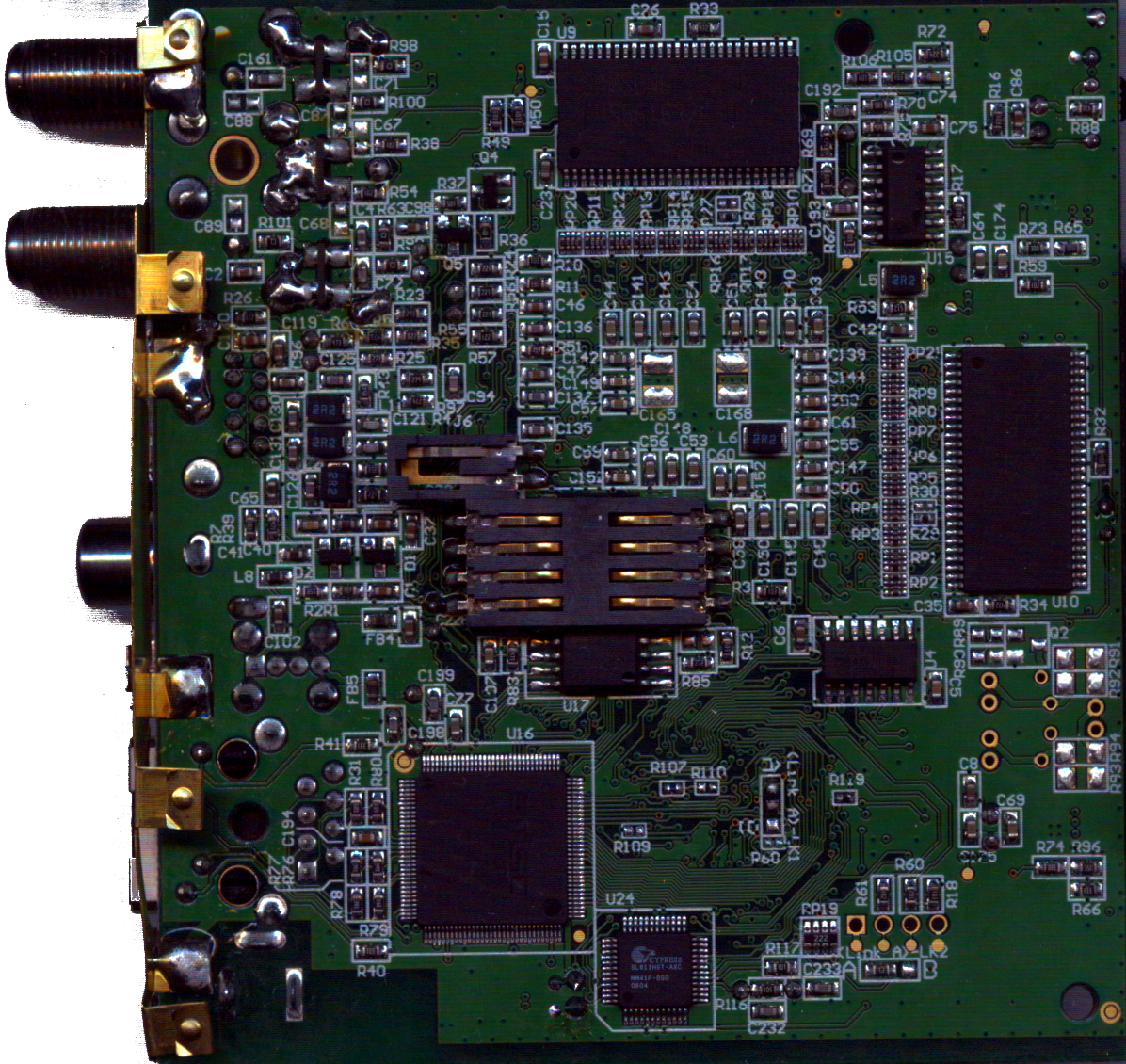
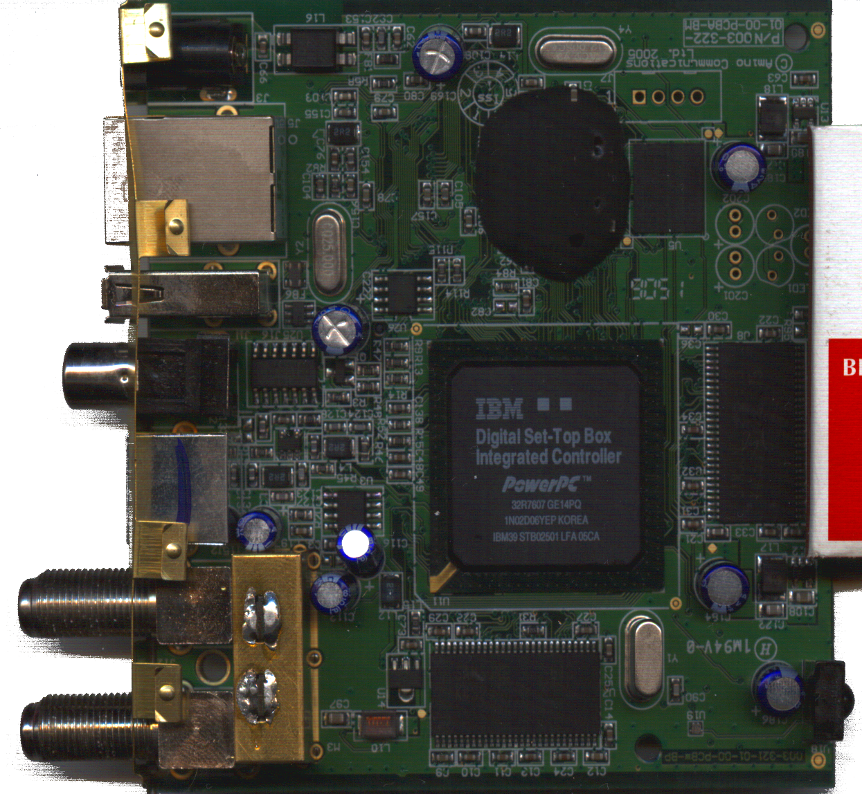
Amino Aminet 110 PCB
These pictures were scanned from my Amino Aminet 110 PCB.


Processor: IBM STB02501 252 Mhz SOC with Powerpc core.
RAM: four 32 MByte K4S561632E chips gives 128 MB integrated RAM.
FLASH: K9F5608UDD 32 MB Flash chip
USB controller: SL811 USB 1.1 host/slave controller
Ethernet PHY: LAN91C113 10/100 Ethernet Phy
There is an IC lying under the smart card connector pins. Possibly I will desolder it, to find out it's name.
There is a BGA IC near the flash what is melted with glue. This could be possibly something like a Macrovision decoder IC. I guess this is melted with glue because the manufacturer wanted to make reverese engineering harder.
The J7 (4 pin unpopulated connector) is a serial port.
Pinout:
PIN 1 (square) - VCC
PIN 2 - TX
PIN 3 - RX
PIN 4 - GROUND
Output from the serial console (without multicast server):
Initialising NOR Flash.

Amino Communications IntActOS-32 v1.44 on AMINET11x with 64Mb RAM
Processor: 51510950  running at 252.000 MHz

00140000 ASB v1.22
00148000 FIL v1.36
00150000 VUL v1.14
00158000 ETH v1.26
00168000 CPT v1.00

AMINET11x BOOT ROM VERSION 1.32.14
TV system = PAL-I Output format = CVBS-RGBON
Setting DENC0_CR1 to 91000040
Setting DENC1_CR1 to 91001F40
Setting DENCMUX to 3E000000
iic write status: 00000000
multicast booting
PHY=LAN83C183 (LAN91C111 Internal)
SMC91C11xFD(rev:2) at 70100300  IRQ:25 MEMSIZE:8192 ADDR: 00:02:02:0D:FF:E0
PHY auto-negotiate timed out
flashled: major=00000001 , minor=00000001

bootos AMINET.img


